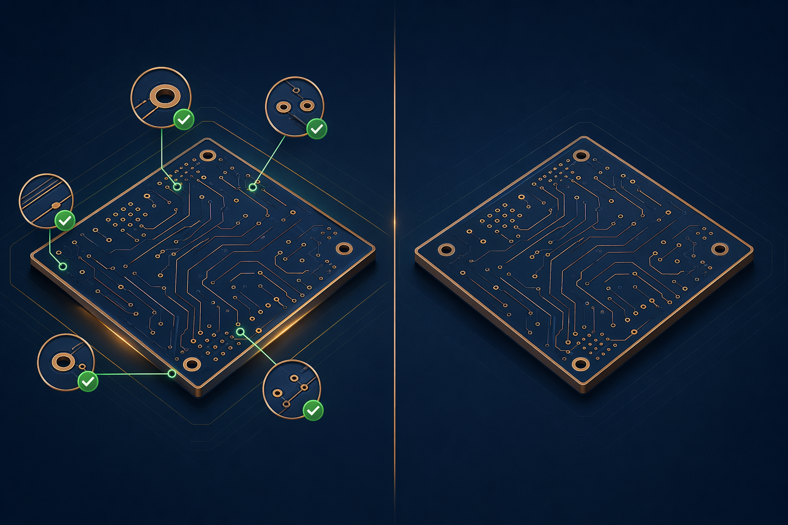
What Is DFM and Why Does It Matter?
Design for Manufacturability (DFM) is the practice of designing a printed circuit board in a way that makes it easy to manufacture consistently, at high yield, and at reasonable cost. A PCB layout that passes electrical DRC checks can still be a manufacturing nightmare — requiring special fixtures, slowing placement speed, generating excessive defects, or making inspection difficult.
The cost impact of DFM is not theoretical. A board with poor panelization that wastes 30% of the panel area adds 30% to the per-unit cost of every component placed, every solder joint formed, and every inspection cycle. Getting DFM right early — before Gerber files are frozen — is the single highest-leverage investment a product team can make in production economics.
Panelization: V-Score vs Tab-Routing
Panelization is the process of arranging multiple copies of your board on a single production panel. The panel format determines how boards are handled through every machine on the line — stencil printer, pick-and-place, reflow oven, and depanelization.
The two dominant methods are V-score and tab-routing. V-score cuts a V-shaped groove approximately one-third of the way through the board from both sides, leaving a thin web of material that can be broken cleanly after assembly. It is inexpensive and fast, but it only works for straight-line cuts across the full panel — boards must be rectangular and aligned. Tab-routing uses a router to cut most of the board outline, leaving small tabs (typically 1.6 mm to 2.0 mm wide) that hold the board in the panel. Tab-routing supports any board shape but costs more in tooling time and requires careful tab placement at least 4 mm from any component to avoid mechanical stress during depanelization.
Recommended panel size depends on your assembler's line capacity, but 250 mm by 300 mm is a widely compatible standard. Leave at least 5 mm rail clearance on each long edge for conveyor transport, and place tooling holes (3.2 mm diameter) in each corner of the panel rail for fixturing alignment.
Component Placement: Keepout Zones, Clearance, and Fiducials
Component placement directly affects placement speed, solder joint reliability, and inspection access. Three rules deserve special attention.
Edge Clearance
Maintain a minimum 3 mm component-to-board-edge clearance. Components placed closer than 3 mm to the edge risk damage during depaneling and are difficult for wave soldering fixtures to shield. For connectors with mechanical insertion force, extend this to 5 mm to allow adequate fixture support.
Keepout Zones
Every fine-pitch IC needs a keepout zone around its perimeter — typically 2 mm to 3 mm — free of tall components that would block the placement nozzle or inspection camera line-of-sight. Tall electrolytic capacitors, transformers, and connectors should never be placed between a BGA or QFP and the nearest board edge, because they shadow neighboring joints from AOI inspection lighting.
Fiducial Marks
Fiducial marks are the reference points that pick-and-place machines use to locate your board in space. Place three global fiducials (one in each corner of the board outline, not the panel rail — board-level fiducials compensate for panel distortion independently). For fine-pitch components (0.5 mm pitch or tighter), add two local fiducials diagonally opposite each other, within 5 mm of the component body. A typical fiducial is a 1.0 mm diameter copper pad surrounded by a 2.0 mm solder mask clearance, with no copper pour or traces in the clearance zone.

Solder Mask and Paste: Pad Design Rules
Solder mask clearance — the gap between the copper pad edge and the solder mask opening — should be at least 0.1 mm (4 mils) to account for mask registration tolerance. Tighter clearances risk mask encroachment onto the pad, reducing the solderable area and weakening the joint.
Stencil thickness governs the volume of solder paste deposited. For most SMT work, a 0.1 mm (4 mil) to 0.15 mm (6 mil) stainless steel laser-cut stencil is appropriate. Use 0.1 mm for fine-pitch (0.4 mm to 0.5 mm) components to avoid paste bridging, and 0.15 mm for power packages or connectors that need a larger solder volume. For mixed-technology boards with both fine-pitch and power components on the same side, a step stencil (varying thickness across zones) can optimize paste volume selectively.
BOM and CPL Data: The Paper Trail That Makes or Breaks a Build
A complete, accurate Bill of Materials and Component Placement List is as important as the Gerber data. Every line in the BOM must have a verified manufacturer part number (MPN) — not just a description. Use the manufacturer's current part number, not a distributor SKU, because the latter can change when distributors update their internal catalogues. Specify at least one approved alternate MPN for every part that is not a generic passive (resistors, capacitors) or diode, and verify that alternates are not marked obsolete by the manufacturer.
The CPL file (also called Pick-and-Place or Centroid file) must include: designator (e.g., R12, U3), X/Y coordinate in millimeters from the board origin, rotation per IPC-7351 convention, and side of board (Top or Bottom). The board origin — usually the lower-left corner — must match exactly between the Gerber and the CPL. A mismatch of even 1 mm produces a completely unusable placement. Always specify the coordinate format (e.g., "millimeters, leading-zero-suppressed") in your documentation package.
DFM Checklist Summary
Use this checklist before releasing your design to production. Each item represents a real failure mode we have observed on the line.
| DFM Rule | Recommendation |
|---|---|
| Panel size | 250 mm × 300 mm standard; leave 5 mm rail clearance each long edge |
| Edge clearance | 3 mm minimum component-to-edge; 5 mm for connectors |
| Fiducials | 3 global per board; 2 local per fine-pitch IC (within 5 mm of body) |
| Solder mask clearance | 0.1 mm (4 mils) minimum from pad edge to mask opening |
| Stencil thickness | 0.1 mm for fine-pitch; 0.15 mm for power; step stencil for mixed |
| BOM MPN | Verified manufacturer part number; at least one approved alternate per critical part |
| CPL coordinates | Millimeters; origin matches Gerber; include designator, X, Y, rotation, side |
| Keepout zones | 2-3 mm around fine-pitch ICs; no tall parts between IC and board edge |
Conclusion: Early DFM Review Saves Cost at Every Stage
The most expensive DFM problem is the one discovered after stencils are cut and reels are loaded. A thorough review before Gerber release catches issues while they cost nothing to fix. At Uppcba, we provide a free DFM review with every quotation — our engineers examine your Gerber files, BOM, and CPL data against the same checklist we use for our own production, and we flag potential issues with specific, actionable recommendations before a single tool is prepared.
Submit your design for review. The DFM feedback you receive today is the rework you will never have to pay for tomorrow.