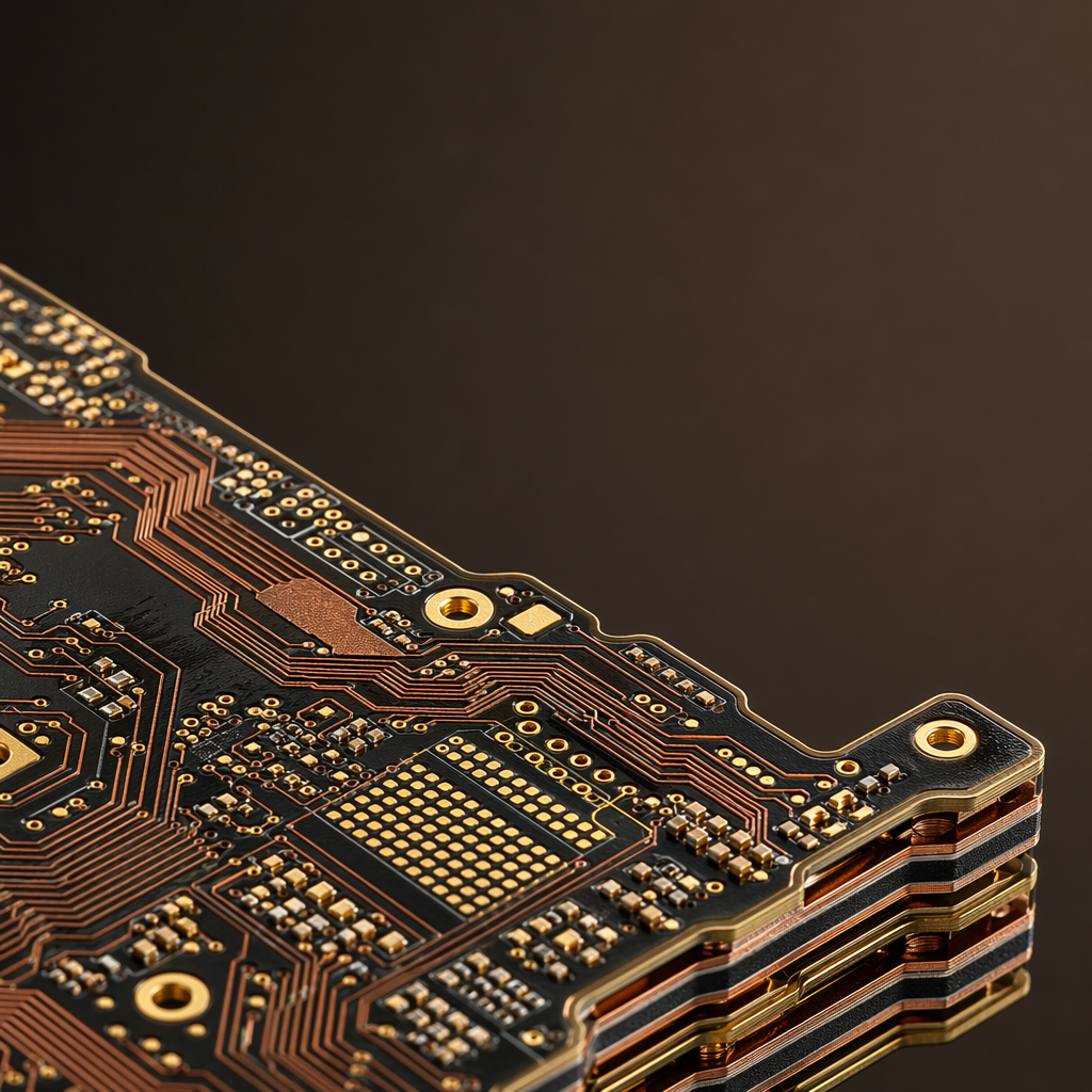
PCB manufacturing capabilities

Precision PCB Fabrication

2–32 layers. 2.5/2.5 mil trace/space. HDI any-layer. 80,000㎡ monthly capacity.

Manufacturing Capabilities

ParameterStandard CapabilityAdvanced Capability
Layer Count2-16 layers18-32 layers
Board Thickness0.4mm - 3.2mm0.2mm - 6.0mm
Min Trace / Space4/4 mil2.5/2.5 mil (HDI)
Min Hole Size (Mech)0.25mm0.15mm
Min Hole Size (Laser)0.10mm0.075mm
Impedance Control±10%±5% (premium ±3%)
Copper Weight1oz - 3oz0.5oz - 12oz
Aspect Ratio10:116:1
Solder Mask ColorGreen, Blue, Red, Black, White, Yellow, Purple, Matte Green, Matte Black
SilkscreenWhite, Black, Yellow
Min BGA Pad0.35mm0.25mm

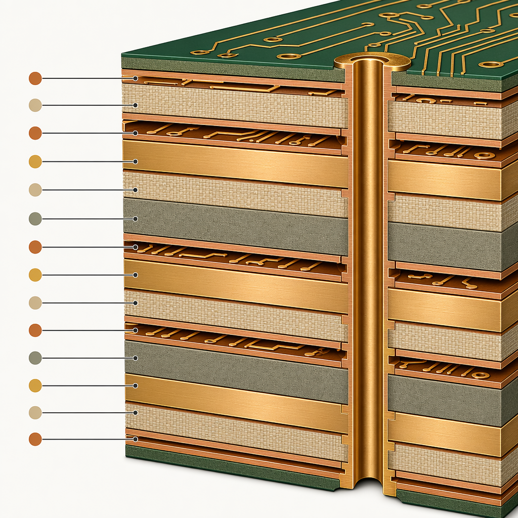
Multi-Layer PCB Stackup

From simple 2-layer to complex 32-layer HDI with blind & buried vias.

PCB cross-section layer diagram

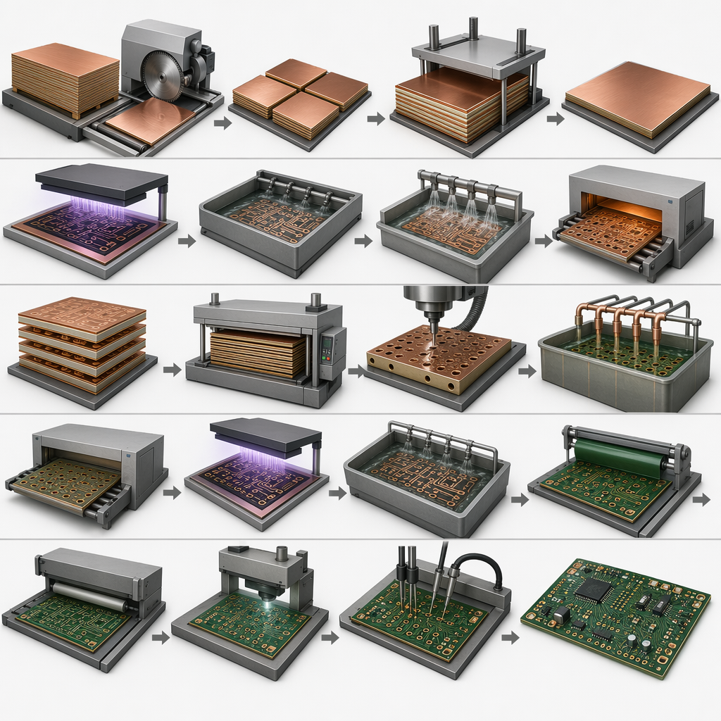
From Gerber to Finished Board

PCB manufacturing process flow
1
CAM Engineering
DFM review & panelization
2
Inner Layer
LDI exposure, DES, AOI
3
Lamination
Multi-layer press bonding
4
Drilling
Mech + laser drilling
5
Plating
PTH & pattern plating
6
Outer Layer
LDI, DES, AOI
7
Solder Mask
LPI, UV cure
8
Surface Finish
ENIG, OSP, HASL, etc.
9
Testing
Flying probe, impedance

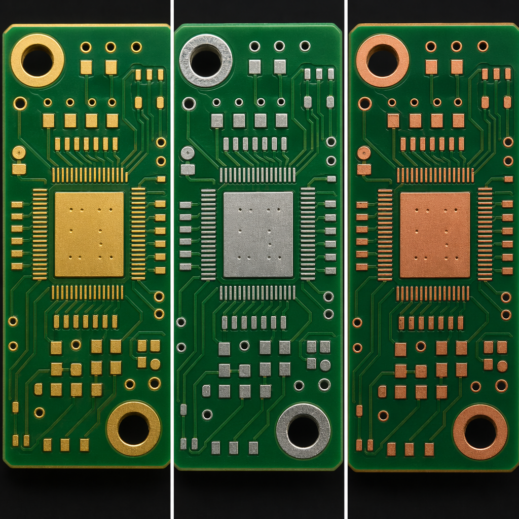
8 Finish Options for Every Application

PCB surface finish comparison

ENIG

Gold over Nickel — best solderability, flat surface

ENEPIG

Gold over Palladium over Nickel — wire bonding

HASL Lead-Free

Tin-Copper-Silver — RoHS compliant, cost-effective

Immersion Silver

Silver coating — RF/high-frequency, smooth surface

Immersion Tin

Tin coating — fine pitch, flat pads

OSP

Organic coating — cost-effective, RoHS, short shelf life

Hard Gold

Thick gold — edge connectors, high durability

HASL

Tin-Lead — legacy applications, excellent solderability

Substrate Options

Standard FR-4 to advanced high-frequency laminates.

Standard Materials

  • FR-4 (Standard Tg 130-140°C)
  • FR-4 (High Tg 170-180°C)
  • FR-4 (Halogen-Free)
  • CEM-1 / CEM-3
  • Aluminum (1W - 3W/mK)

Special Manufacturing Capabilities

HDI Any-Layer
Sequential lamination with laser microvias. Any-layer interconnect for maximum density and routing flexibility in complex designs.
Blind & Buried Vias
Precision depth-controlled drilling for layer-to-layer connections without consuming surface routing space.
Back Drilling
Remove unused via stubs on high-speed signals. Reduce signal reflection and improve signal integrity for 5G and RF designs.
Via-in-Pad
Fill and plate-over vias located in SMD pads. Maximize component density. Compatible with 0.4mm pitch BGA and below.
Edge Plating
Copper metallization on board edges for grounding, shielding, and edge connector applications.
Impedance Control
Precision trace width/spacing calculation. TDR verification on every controlled-impedance order. ±5% standard, ±3% available.

Start Your PCB Order

Upload your Gerber files. Free DFM check. Quote within 24 hours. Prototype in 3 days.

Get PCB Quote →